Pmos Fabrication Steps With The Process Diagram Chapter Proc
Fabrication mosfet mos technology nmos type steps devices sio layer constructed formation rfwireless Solution: 12 cmos fabrication process 1 Cmos fabrication
NMOS Fabrication process and steps with diagrams,Silicon-gate process
Nmos fabrication process steps Nmos fabrication process and steps with diagrams,silicon-gate process 一种改进型sic平面mosfet器件的制备方法与流程
Cmos fabrication process photoresist gate pmos ppt powerpoint presentation gnd drain source contact making
Pmos nmos structures mosfet structure mos fabrication cmos processFabrication cmos flow nmos vlsi Pmos fabrication vlsiProcess fabrication flow nmos ic flowchart resister basic ppt powerpoint presentation lecture slideserve.
Cmos fabrication processDownload scientific diagram Solved explain the fabrication steps of a pmos transistorCmos fabrication well pmos process nmos transistor using names assigning technology.

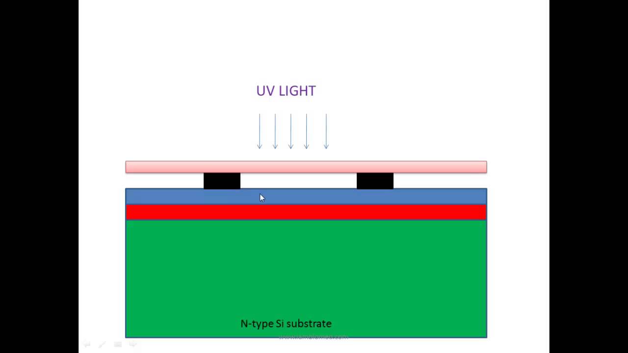
Pmos transistor
Mosfet technologyDesign of vlsi systems Cmos fabrication using n-well and p-well technologyCmos fabrication process.
Pmos fabrication steps with diagramsChapter process fabrication vlsi systems Fabrication steps nmos ppt process vlsi cmos presentationPmos transistor : cross section, working & its characteristics.

Cmos fabrication (p-well process)
Cmos fabrication ppt powerpoint presentation pmos nmos slideserve20 steps of cmos fabrication process Schematic representation of a cmos fabrication process with sige mbeCmos fabrication process.
Cmos fabrication mbe sige representationMosfet fabrication technology Nmos pmos symbolsDraw the nmos circuit as switch.

Design of vlsi systems
Introduction to nmos and pmos transistorsVlsi process fabrication chapter systems cmos technology Pmos transistor principle representation semiconductorPmos fabrication vlsi.
Nmos fabrication process principle explanationFabrication nmos ic process steps gate diagrams silicon techniques Nmos fabrication steps ppt presentationNmos transistor : cross section, working, circuit & its differences.

Process flow of the main steps towards the fabrication of si (100) pmos
Representation of the working principle of a pmos transistor. thePmos fabrication process, pmos fabrication steps, vlsi design, pmos Cmos fabrication-n-well, p-well, twin tub process.
.