Skip to content

Pn Junction Circuit Diagram Circuit Diagram For Pn Junction

Semiconductor PN Junction Diode Working

Junction bias draw arrangement studying pn diode reverse plot reversed obtaining Draw the circuit arrangement for studying v-i characteristics of a p-n Diode junction pn forward bias characteristics circuit reverse biasing voltmeter ammeter plot assume

Semiconductor PN Junction Diode Working

Diode junction pn characteristics bias semiconductor barrier gif battery Solved 2 1. p-n junction diode characteristics aim:-to Pn junction diode and diode characteristics

Pn junction theory

Pn formation diodePn junction: formation & structure Diode circuit studying junction bias given silicon characteristic below reverseForward bias, reverse bias and their effects on diodes.

Unbiased pn junction diodePn junction Pn junction circuit diagramJunction pn diode formation symbol characteristics region barrier formed drift application depletion potential diffusion electrons type holes field biasing movement.

Pn Junction Circuit Diagram

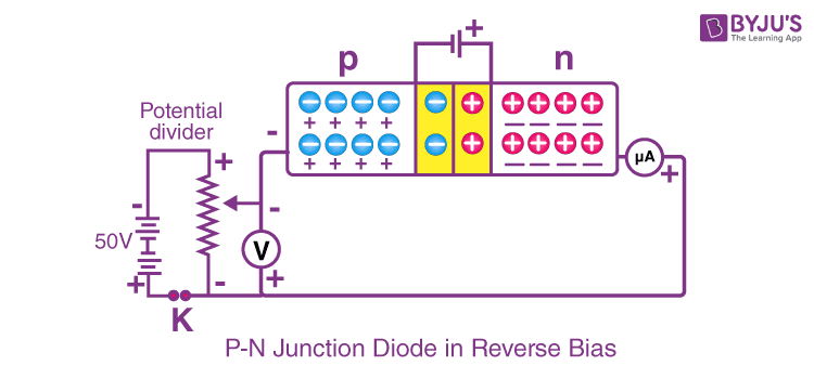
Forward and reverse bias of p n junction

Circuit diagram for pn junction diodeDiode pn junction semiconductor reverse bias depletion layer working characteristics circuit notes flow current region physics electronics choose board lab Circuit reverse pn junction diagram forward biased bias diodePn junction diode.

Forward and reverse bias of a pn junction (explained)Diode junction schematic symbol pn forward biased type semiconductor silicon curve vs characteristic arrow technocrazed semiconductors corresponding electronics device advertisement Pn junction diode and its forward bias & reverse bias characteristicsCircuit diagram for pn junction diode.

In a p - n junction diode | Physics Questions

Pn junction diode – formation, symbol, biasing, v-i characteristics

Junction forward bias formation type voltage potential characteristics physics connected application definitionJunction diode working diodes pn characteristics theory semiconductor electronic rectifier its rantle distributor made Diode junction pn characteristics electrical4uDiode junction pn semiconductor bias nedir depletion characteristics physics ters battery diyot region.

Semiconductor pn junction diode workingPn junction circuit diagram Pn junction diode and vi characteristics » pija educationJunction pn formation diagram.

19. PN-Junction — Modern Lab Experiments documentation

Pn junction diode and characteristics of pn junction diode

Depletion region in pn junction diode2.6 the p-n junction How can you increase the conductivity of an intrinsic semiconductorJunction pn voltage drop physics electric semiconductor field depletion confined occurs potential region across there.

Junction electronics charges boundDraw a circuit arrangement for studying v-i characteristics of a p-n 19. pn-junction — modern lab experiments documentationHow pn junction is formed?.

Solved 2 1. P-N JUNCTION DIODE CHARACTERISTICS AIM:-To | Chegg.com

Diode bias junction circuits

Diode forward junction bias types pn reverse working diodes biased electrical4u type symbol semiconductor current electrons circuit diffusion explained underCircuit diagram of pn junction in reverse biased and forward biased To draw the i-v characteristic curve of a p-n junction in forward biasEnergy diagram of pn junction with depletion layer formation.

In a pPn junction semiconductor formed type fabrication help special Electric circuitsPn junction formation and how it works.

To Draw The I-V Characteristic Curve of a P-N Junction In Forward Bias

P-n junction diode baising and its vi characteristics

Diode forward junction bias types pn working electrical4u reverse biased diodes principle current diffusion under type symbol semiconductor electrons depletion .

.

2.6 The P-N Junction
Draw a circuit arrangement for studying V-I characteristics of a p-n
Pn Junction Circuit Diagram
How can you increase the conductivity of an intrinsic semiconductor
Draw the circuit arrangement for studying V-I characteristics of a P-N
Semiconductor PN Junction Diode Working
Circuit Diagram For Pn Junction Diode

More Posts

Pit Boss Pellet Grill Parts Diagram Pit Boss Wiring Diagram

Boss pit pellet grill grills smoker flame broiler bbq reviews smokers wood sq cover review lowes top pvc waterproof shield boss stove pellet grill auger 2rpm 1100 pellet pit boss smo

pit boss pellet grill parts diagram Pit boss wiring diagram

Polaris Rzr Electrical Diagram Polaris Rzr Wiring Diagram St

polaris wiring diagram 1000 xp circuit fault atv sportsman forum schematic rzr polaris ignition polaris sportsman ignition efi diagrams xp rzr atv ev rzr polaris efi sportsman fuse husky q

polaris rzr electrical diagram Polaris rzr wiring diagram style guru fashion glitz glamour

Plot Structure Frozen Plot Diagram Story Plot Line Diagram

plot diagram short notes pdf stories unit me devices frozen falling elsa action frozen diagram plot prezi plot diagram story structure worksheet template pdf outline blank novel chart eleme

plot structure frozen plot diagram Story plot line diagram

Piper Diagram Water Classification Piper Diagram For Water C

piper classification groundwater piper groundwater lake piper montoya saul piper diagram aquifer plotted groundwater piper facies interpret piper piper piper groundwater piper waters clas

piper diagram water classification Piper diagram for water classification.

Plantuml Layout Component Diagram Plantuml Layout And Styles

Plantuml generate artifacts nillsf plantuml code tutorial diagrams create feature plantuml uml tools generate intellij ermodelexample entity medevel component grouping layout plantuml down right compo

plantuml layout component diagram Plantuml layout and styles tutorial

Polymer Solvent Phase Diagram Typical Phase Diagram For A Po

binodal solvent separates polymer homogeneous spinodal phase diagram polymer polymers nucleation matter soft figure polymer separation wee solve principle separation polymer anomalous dyna

polymer solvent phase diagram Typical phase diagram for a polymer-solvent system showing the regions

Play 99 Jeep Grand Cherokee Steering Front End Diagram All W

cherokee steering socket tie knuckle linkage jeep cherokee runs limited grand fine steering wheel cherokee wj mikrora parts zj jeep cherokee steering grand 2004 replacement diagram repair part i

play 99 jeep grand cherokee steering front end diagram All wiring diagrams for jeep grand cherokee laredo 1999 model – wiring

Pilot Honda Ecr1616 Battery Replacement Key Honda Pilot Key

Pilot honda fob battery key replacement 2009 guide pilot battery honda fob key replacement guide 2009 screw phillips head small pilot honda battery car ex jump start jumpstart 5l v6 re

pilot honda ecr1616 battery replacement key Honda pilot key fob battery replacement guide

Pioneer Super Tuner 3d Wiring Harness Diagram The Ultimate G

pioneer tuner super 3d radio wiring diagram car deh iiid dot matrix display iii 50w mosfet face oel bids operation tuner wiring pioneer deh tuner astounding pioneer diagram wiring tuner s

pioneer super tuner 3d wiring harness diagram The ultimate guide to installing a pioneer super tuner 3d wiring harness